LO1 Explain and analyse simple combinational logic circuits
Map. P1 Explain and analyse the operation of a simple combinational logic circuit, making limited use of Truth Table, Boolean Algebra and Karnaugh Map.
M1 Analyse and optimise the operation of a combinational logic circuit making good use of Truth Table, Boolean Algebra and Karnaugh Map.
D1 Analyse, optimise and enhance combinational logic circuits, making best use of Truth Table, Boolean Algebra and Karnaugh
LO2 Explain and analyse simple sequential logic circuits
. P2 Explain and analyse the operation of a simple sequential logic circuit, making use of Timing Diagrams.
M2 Analyse and optimise a simple sequential logic circuit, making use of Timing Diagrams.
D2 Analyse, optimise and enhance a sequential logic circuit, making use of Timing Diagrams
LO3 Describe and evaluate the technologies used to implement digital electronic circuits
P3 Apply lab equipment to describe and evaluate simple digital circuits.
M3 Apply lab equipment to configure and test simple digital circuits.
D3 Apply lab equipment to configure, test and evaluate digital circuits, comparing and evaluating characteristics of different technologies.
LO4 Describe and analyse a range of digital subsystems, hence establishing the building blocks for larger systems
P4 Describe and analyse the principles of a range of different logic subsystems.
M4 Describe and analyse a range of different logic subsystems, indicating the place they might take in a larger system.
D4 Describe and critically evaluate a range of different logic subsystems, comparing these with other techniques or subsystems available, indicating the place, they might take in a larger system.
Do You Need Assignment of This Question
Assignment Questions:
Q1. (Learning Outcome 1)
Explain, analyze, optimize, and enhance the operation of a simple combinational logic circuit with three (03) fail-safe sensors and one (01) emergency shutdown switch. The line should keep moving unless any of the following conditions arise:
- If the emergency switch is pressed, the system shuts down.
- If sensor 1 and sensor 2 are activated at the same time, the system shuts down.
- If sensor 2 and sensor 3 are activated at the same time, the system shuts down.
- If all sensors are activated at the same time, the system shuts down.
A. Explain, analyze, and optimize the operation of the combinational logic circuit: In order to do this,
1. Construct the truth table for the above scenario.
2. Derive the Boolean expression (un-simplified) for the system shutdown conditions.
3. Simplify the Boolean expression using a Karnaugh Map.
4. Implement the digital logic circuit for the simplified expression using:
1. AND, OR, and NOT gates
2. Only NAND gates
3. Only NOR gates
Use appropriate variables and write down any assumptions made during the circuit implementation.
B. Enhance the combinational logic circuit by providing two advantages of simplifying Boolean expressions rather than implementing them in the un-simplified format.
Q2. (Learning Outcome 2)
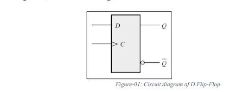
1. Explain the operation of the D flip-flop as a simple sequential logic circuit.
2. Given the D flip-flop circuit in Figure-01 and the input waveforms for D and CLK in Figure-02, answer the following:


a. Analyse and determine the output waveforms for both the Q and Q̅outputs for all six clock pulses given. Complete the table below, stating all your assumptions and workings related to the answer:

Buy Answer of This Assessment & Raise Your Grades
b. Construct and optimize the resulting waveform for the Q and Q̅outputs based on the input waveform given in Figure-01. Identify any setup and hold time violations using the Timing Diagrams and propose adjustments to the D input transitions to avoid these violations. Illustrate these changes in a revised Timing Diagram.
c. Enhance the sequential logic circuit by discussing the benefits of the proposed optimizations and their impact on the circuit’s performance and efficiency.
Q3. (Learning Outcome 4)
A. Certain digital equipment used in a medical laboratory consists of 128KB (Kilobytes) of main memory for storing information & data. The processor fetches and writes the data to and from the main memory. Main memory has the following characteristics.
Memory is divided into memory locations (memory cells), which each location can hold one byte.
- Each memory location must be addressable individually.
- Each memory location has a unique memory address. The processor of the equipment uses an address decoder for communicating with the main memory.
I. Describe the function of an address decoder in between the processor and the main memory. Analyze why this function is critical for memory access.
II. Calculate how many input lines (address lines) should be necessary in minimum when the processor wants to address the entire memory.
III. Draw the block diagram of the decoder which is used in the medical equipment. Mention the type of decoder into format of N-to-M decoder.
B
. I. Describe the general concept of encoding something.
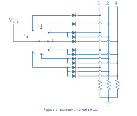
II. The digital encoder depicted in this diagram utilizes a basic configuration of switches and diodes. Describe the function of this circuit as the switch is switched between various positions. Analyze how the encoder output might be used in a larger digital system.

III. Based on the truth table below, determine which diode has failed in the circuit. Please note that the table represents the actual behavior of the encoder circuit, not what it’s supposed to do.
IV. Analyze how a Multimeter can be used to identify a malfunctioning diode in the circuit. Explain the rationale behind the forward and reverse bias testing procedures, and how the readings on the Multimeter help determine the state (good or bad) of the diode.
V. Critically evaluate the limitations of using a simple encoder circuit like the one shown in the diagram (Section B.II) compared to alternative encoding techniques. Briefly mention a possible alternative and its advantages.
Are You Looking for Answer of This Assignment or Essay
The post BTEC Unit 20: Explain, analyze, optimize, and enhance the operation of a simple combinational logic circuit with three (03) fail-safe sensors and one (01) emergency shutdown switch- Digital Principles Assignment 1, UK appeared first on Students Assignment Help UK.